Basic Z80 Microcomputer
I’ve wanted a little Z80 microcomputer of my own for ages. I never learned to get the most out of a Z80 when it was appropriate (like, when I had a Spectrum +2) and it seemed simple enough to build on my own. There’s a smattering of other Z80 self-builds on the Internet and a fantastic free book about the process.
I chose the Z80 because:
- It’s close to the 8086 instruction set, which I’ve been exposed to on-and-off for years.
- It’s still available for purchase.
- It can be clocked very slowly1, so I can use blinking lights and the electronics group’s 10Mhz scope for debugging if I need to.
- IO is not memory mapped. There’s effectively a separate bus for memory and IO operations.
- There’s a tiny pipe dream that I could get CP/M up and running one day.
- I had some experience with the C language toolchain for it.
Not Even Hello World
I ordered a Z80 (6MHz DIP40 version, though it’s never going that fast — Z84C0006PEG) and a 1MHz oscillator (not just a crystal!). I had 8K of flash ROM and 64K of static RAM left over from an earlier project. I got a set of three breadboards to build everything on, an Arduino Mega clone to program it, a little breadboard PSU and a PIO (because it was cheap).
The first step was to get a ‘free running’ circuit working. I followed what Stian Soreng did and pulled the data and address busses down to ground, and NMI/INT/HALT/WAIT and RESET up to 5V. I put an LED (uh, segment) on A11 so that I could see the light flash around every 2048 instructions.
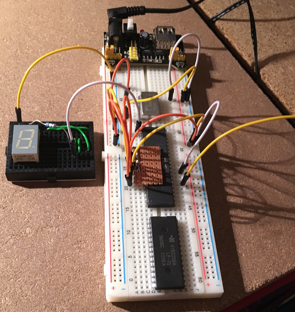
Slowly Slowly
I ended up using a 7493 to divide the clock by 8 so I could slow things down and monitor things with LEDs. This means my Z80 is running at 125KHz.
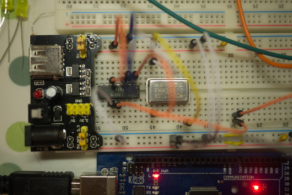
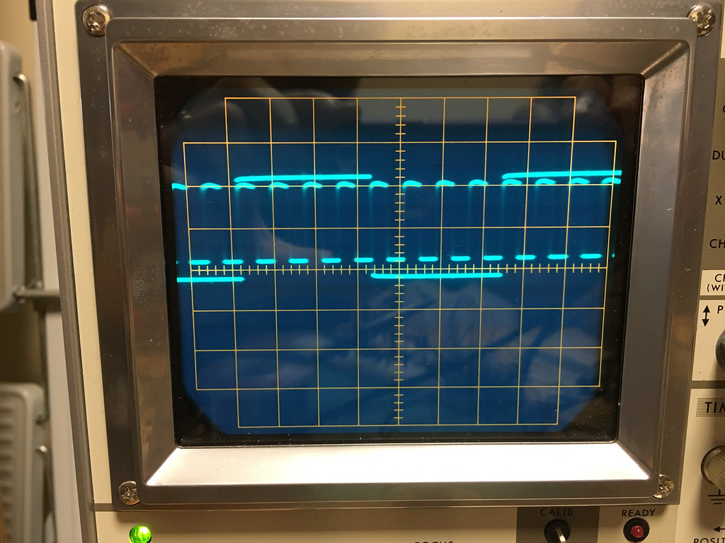
I’m thrilled to say that this worked first time: I’d never used this part and the part itself was highly suspect, but you can see the original and the divided signal on the A and B channels of our oscilloscope:
Learning to Count
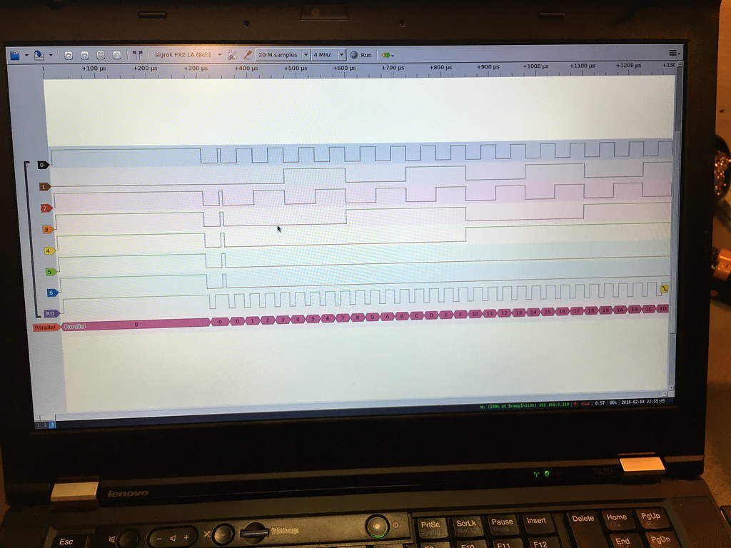
Blinking a light is the Hello World of hardware, but I’d gotten a logic analyser for Christmas (specifically for this project, really). It has 8 inputs, which is more limiting than I originally expected, so I hooked up the lower seven pins to the address bus and a pin to /RD, with a trigger set.
It looks beautiful at this point:
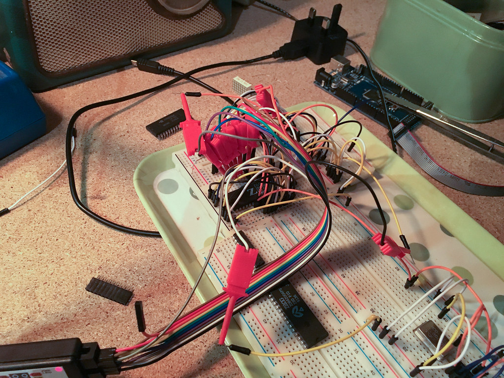
But at least you can see it counting! I’m going to consider this as a program
which is all NOP instructions is just another way for saying “incrementing
PC”.
Programming
Well, now that we can definitely execute NOPs, it would be great to execute
even a small program. It turns out that this simple step requires a pretty
considerable amount of work. There’s a hint in the last update’s pictures,
where you can see my Arduino Mega (clone) in the background.
The idea was always to get the Arduino to poke some data into the RAM and then start the processor. In the early stages that can mean I avoid programming flash ROMs, which is a whole extra level of messing around I’d love to short circuit. This adds many wires.
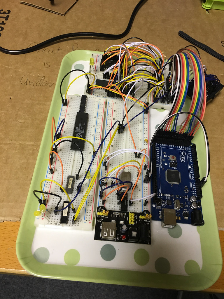
I’m breaking with chronology here: I wrote the RAM programmer before the Z80’s arrived, so I could be reasonably sure that this approach would work. The earliest version just wrote a values to matching RAM locations and read it back out again - you can see that here.
The better version actually responds to commands:
- (d)ump the contents of the bottom 256 bytes of RAM
- (z)ero the RAM, for sanity
- (l)oad the preconfigured program, stored in the microcontroller
- p(o)ke one memory location
I’ll deal with poke in a later update, but this program, and the example
program encoded in ram[] lets me zero the RAM, load in the program, bring
the RESET line high on the processor, wait a second, bring RESET low, and
dump the RAM out.
Here’s the RAM after a triumphant run:
0x00 00 FF D3 55 D3 55 18 F8  55 14 7A D6 C8 38 F3 18
0x10 EF 00 00 00 00 00 00 00  00 00 00 00 00 00 00 00
That’s the program itself.
0x20 00 00 00 00 00 00 00 00  00 00 00 00 00 00 00 00
0x30 00 00 00 00 00 00 00 00  00 00 00 00 00 00 00 00
0x40 00 00 00 00 00 00 00 00  00 00 00 00 00 00 00 00
0x50 00 00 00 00 00 B1 00 00  00 00 00 00 00 00 00 00
There’s some data I wrote to IO 0x55. A little hiccup: because I haven’t done
any address decoding on this board yet, OUT instructions actually write RAM.
0x60 00 00 00 00 64 65 66 67  68 69 6A 6B 6C 6D 6E 6F
0x70 70 71 72 73 74 75 76 77  78 79 7A 7B 7C 7D 7E 7F
0x80 80 81 82 83 84 85 86 87  88 89 8A 8B 8C 8D 8E 8F
0x90 90 91 92 93 94 95 96 97  98 99 9A 9B 9C 9D 9E 9F
0xA0 A0 A1 A2 A3 A4 A5 A6 A7  A8 A9 AA AB AC AD AE AF
0xB0 B0 B1 B2 B3 B4 B5 B6 B7  B8 B9 BA BB BC BD BE BF
0xC0 C0 C1 C2 C3 C4 C5 C6 C7  00 00 00 00 00 00 00 00
And here’s a simple “write A to the memory location A” style effect: 0x64 contains an 0x64 and so on.
The program was written in C, here’s the full listing. I’ll switch to assembly for the next few programs, because it’s easier for me to verify my programs and learn about the different addressing modes that the processor supports in assembly.
Assembly
The equivalent to the above C program is this short commented Assembly
listing. My first draft of address decoding hadn’t worked, so I wanted to
go back and check that even the /IO pin was being toggled in the way that I
expected.
I’d already found that hooking up my logic analyser was leading to weird results, so I opted to try my little single-channel kit oscilloscope:
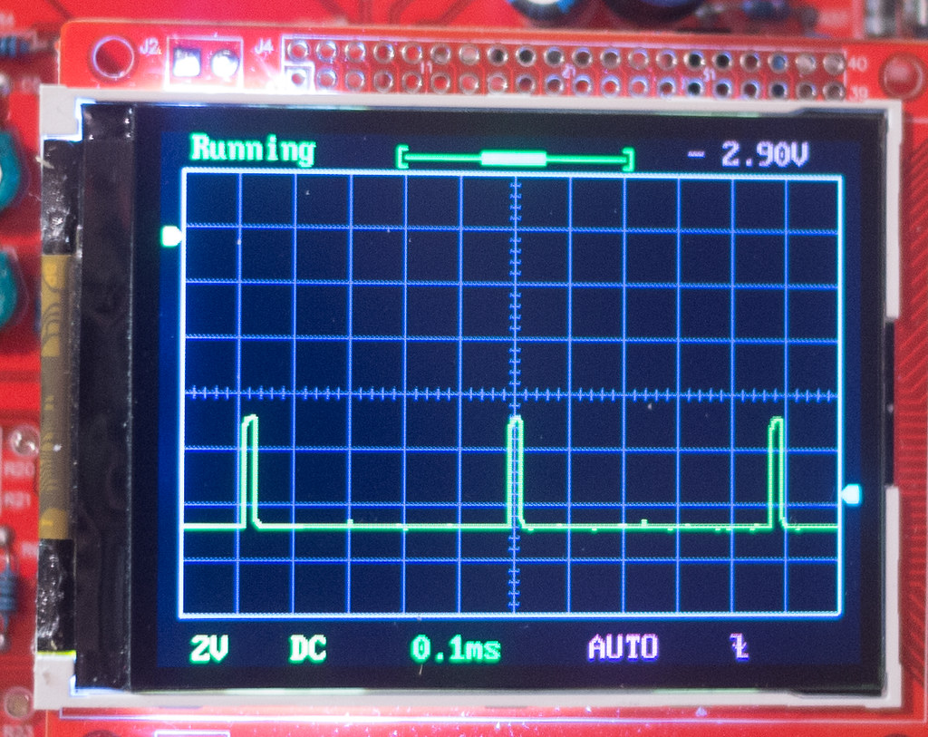
So, 0.5ms apart when running at 125Khz, about 60 clock cycles per IO.
This listing with two IOs, one after another should show me how fast I can toggle the line, without any extra accesses or comparisons:
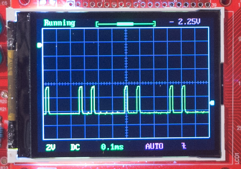
About 12 clock cycles per IO, or 10Khz.
Address Decoding
It’s clearly not great to have IO operations also twiddle bits of RAM.
About the simplest decoding I can do is to join the /CE pin of the RAM to
the /MREQ line of the processor, but even with this done I wasn’t getting
the results I expected.
Most of this was a software fix. I’ve changed the /OE, /WE and
/CE lines to use the internal pull-up resistors (so I’ve removed the 1K’s I
put on the breadboard) and most importantly I’m de-asserting /CE with every
call to disownBus - holding it low the whole time was the source of my
problems.
Now that is done,
0x50 00 00 00 00 00 A1 00 00 00 00 00 00 00 00 00 00
has become the much better
0x50 00 00 00 00 00 00 00 00 00 00 00 00 00 00 00 00
after the program has executed.
Actual IO
To do anything remotely useful with this computer I’m going to need some IO. A UART would be ideal, but first things first, just some LEDs I can control from the Z80 would do.
I’m going to skip past the abortive attempts that didn’t work, using a 7475 Quad Latch. What I do have working is a circuit with a 7404 and a 74HC374 Octal Flip-Flop. I’m going to refer to this as a ‘register’ - that may not be 100% correct, but you can only type flip-flop so many times before it becomes silly.
I’m cheating with my address decoding again: as this is the only IO on the
breadboard, I’m not actually decoding the address lines at all, I’m just
triggering the register based on the /IO signal. I don’t even decode /WR or
/RD - so either IO operation would store the contents of the data bus.
The data lines are hooked directly up to the D lines on the register. The clock
signal for the 74HC374 is positive-edge triggered, but the /IO line is
negative-edge triggered, so I pipe the /IO signal into one of the inverters
in a 7404.
Sidebar: I wasted a lot of time before finding out that one of the inverters in the 7404 is broken. Test your assumptions!

I hooked up the logic analyser to D0, D1, the divided down system clock,
/IO and the IO output from the 7404. The /IO is labelled as IO in the
picture, and the IO signal as _IO. Sorry!
This is a successful capture of part of my new blinking lights program
executing. You can see _IO rise periodically - when it does, the contents of
D0 and D1 are copied to the Q0 and Q1 pins of the 74HC374. These are
connected via LEDs to a resistor and then ground.

This is the current state of the IO section of the board. The 7404 is up top, next to the unconnected 7475, with the 74HC374 in the middle. The LEDs are clearly visible, and the rainbow wires leading off to the logic analyser.
I’m going to need some more gates to do sensible decoding, but this is basically enough to do bit-banged SPI. Milestone!
-
That said, modern 6502’s can apparently be clocked down to DC due to a fully static design. Good for them! My Z80 runs at 125Khz - that’s been slow enough so far. ↩